I have an application that reqires high-side switching of nominal 12V (10-15V) from a lead acid battery with an Arduino compatible board. Obviously, the GPIOs of a 3.3 or 5V Arduino can’t accomplish this task alone. This post describes a circuit utilizing two bipolar junction transistors (BJTs) to accomplish switching 15mA of nominal 12V from a 3.3V Arduino GPIO. The switch is non-inverting.
Having no formal training in electronics and limited experience with transistors sent me straight to Google. Transistors have always been mysterious devices that required wizard level skills to use, or so I had always thought. I was determined to demystify these useful devices, and after hours of reading I finally had my “a-ha” moment. There are three modes a BJT can be operating in. Once I realized that, accomplishing my goal was relatively simple.
The Three Modes
The three modes a BJT can be in are off, saturated, and active. Because I only want to use the device as a switch, the active mode can be ignored. Well, not exactly ignored. Avoided may be the more accurate term. I wanted my device to only be in either the off or saturated mode.
Off is simple. It’s off. No current flows between the collector and emitter. That path through the transistor essentially becomes an open circuit. The transistor is off when there is no current flowing into (NPN) or out of (PNP) the base. This is simple to accomplish by making the base and emitter voltage the same.
Saturation is simple when considering an ideal device. Maximum current flows between the collector and emitter. That path through the transistor essentially becomes a short circuit. The transistor is saturated when there is sufficient current flowing into (NPN) or out of (PNP) the base such that increasing that current would not increase the current flow between the collector and emitter.
We don’t live in an ideal world. In the real world, things are slightly more complicated. It doesn’t really become a short circuit; there is some voltage drop between the collector and emitter. What does maximum current mean in the real world? Anything you want? Not really, there is only so much current a device can manage before it burns out. What’s the limit? How much current needs to be at the base to achieve saturation in the real world? The answers to these questions can be found in the datasheet.
The Datasheet
It would be nice if the datasheet simply said how to accomplish things directly. When is anything that simple? As one of my mentors used to say, if it was easy, everyone would be doing it.
What is a datasheet anyway? It is a list of parameters and their values. Or rather, their minimum, maximum and typical values. Some parameters have all three variants, others have two or only one. On top of that, the parameter names are cryptic, with names like hFE and VBE(sat). No wonder I considered it sorcery. How do we get from alphabet soup to a working design?
That becomes significantly easier when the goal to be accomplished is clear and there is an understanding of which parameters impact that goal. In this case, the goal is to put the transistor in the off state when the Arduino digital pin is low, and to put the transistor into saturation when the pin is high.
Now the goal is clearly defined. Which parameters will help achieve it? Those that directly impact the goal are hFE(min), VCE(sat), and VBE(sat). Indirectly, IC(max) will help choose a device that won’t burn out based on how much current needs to be switched.
Keeping the smoke in
Although this value won’t be used in our design calculations, it is important to know the IC(max) when choosing a specific transistor. This value is the maximum collector current, and exceeding it will release the “magic smoke” from the device and ruin your day. Make sure you know how much current you will be asking the transistor to switch, and make sure IC(max) is bigger than that to avoid burning it up.
“Gain”-ing traction
The first useful parameter is the DC current gain. It is listed as hFE on the datasheet, and is also commonly refered to as beta. For the purpose of a switch, we are interested in the minimum possible gain offered by the device. Consider this the worst case gain. Why the minimum? Remember, we are trying to force the transistor into saturation. The gain specifies the proportion of collector current for a given base current. Say the minimum value for hFE is 10. This means for a given base current, the transistor will allow (up to) 10 times that current to flow between collector and emitter. The transistor reaches saturation when this relationship breaks down, in other words when the transistor is allowing the maximum current it can between collector and emitter. Don’t worry about how we’ll know what that maximum is for now. Instead, think about what would happen if the hFE was 20 instead of 10. The transistor would still be saturated. Therefore, we will design the circuit based on the minimum value for hFE, guaranteeing that the transistor will, in fact, reach saturation.
You may have noticed that the relationships governed by the hFE parameter are defined in terms of current and not voltage. That is because bipolar junction transistors (BJTs) are current controlled devices. This will become important later when we work through the math.
Voltage Relationships
Didn’t I just say that BJTs are current controlled devices? Now, right after that, is a section about voltage relationships. What gives?
BJTs are indeed current controlled devices, but what does that mean? It means their behavior is determined by the current flowing through them. Specifically, the output current is determined by the current flowing at the base.
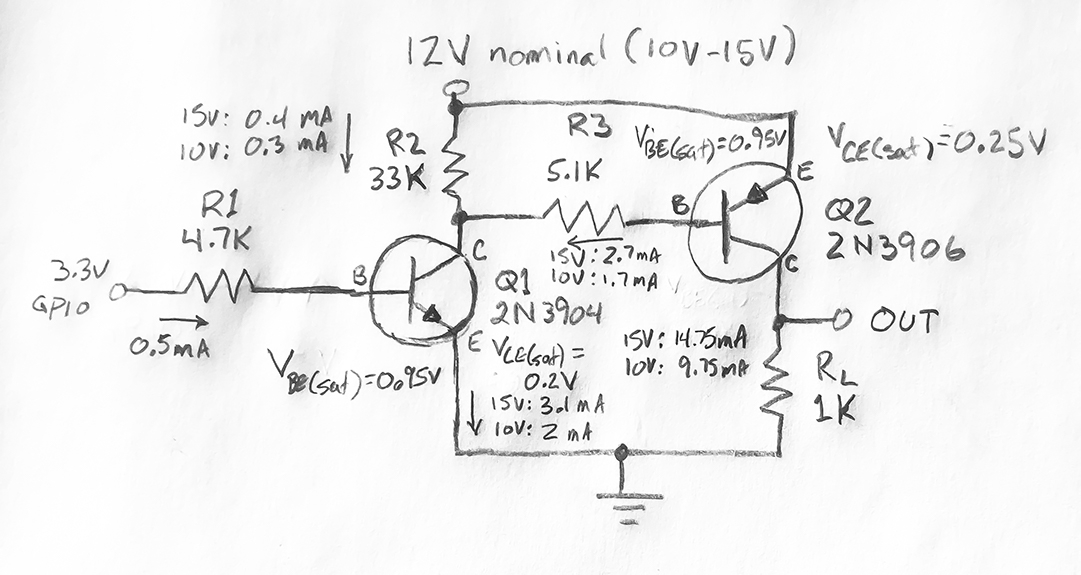
We want to be able to switch nominal 12V on and off using the Arduino, and we want to be able to control a load that draws 15mA. From the circuit diagram, we can see that the output current will flow from the 12V source, through the PNP transistor and then to ground via the load (represented here by RL). The value for this resistor was chosen to create the target output current using Ohm’s law.
We know we have 12V (nominal) from the battery. The actual voltage ranges from 10V to 15V depending on the state of charge (SOC), so we need to calculate for each end of the range. For now, let’s just worry about the high end (15V). Since we know the voltage, we just plug in 15V and 1K ohms into Ohm’s law and turn the crank, right? Wrong.
What? Wrong? Why? To know why it’s wrong, let’s see what would have to be true for it to be right. In order for it to be right, the resistor would have to have 15V across it, meaning the voltage drop between the emitter and the collector would have to be 0V. This would be the case with an ideal transistor, but in the real world it isn’t.
I can almost hear you. “Ok, smarty pants, if it isn’t 0V, then what is it?”
It’s given by the datasheet, by the parameter VCE(sat). This parameter specifies the voltage drop between the collector and emitter when the transistor is in saturation, and is exactly what we need to apply Ohm’s law to the situation. Note that this value is negative for PNP transistors, because as we can see in the circuit diagram the emitter is at a higher voltage than the collector for Q2. For NPN it is positive, and again looking at the circuit diagram we see that the collector is at a higher voltage than the emitter for Q1.
We’re saved! Almost. I bet you’re getting sick of me doing that. I was sure getting sick of it happening when I was trying to understand all this. Like most of the datasheet parameters, VCE(sat) has a range of values. Which one do we use?
To answer that, we go back to the design goals. We want to switch a maximum current of 15mA at 15V. From Ohm’s law, we know that if the resistance is fixed, then the current will go up if the voltage goes up. The voltage (across the resistor) will be at its highest when the voltage drop from the emitter to the collector is at its lowest. Therefore, we will use the minimum value the datasheet provides for VCE(sat) (ignoring the sign). This will guarantee that the output current flow will be 15mA or less.
Now that we have the output current sorted out, we need to determine the base current required to put the transistor into saturation. It took me a while to understand that we only need to get the transistor into saturation for the desired output current, which was typically being called IC(max) in the material I was researching. I was confusing this IC(max) with the maximum collector current from the datasheet, which is 200mA for the 2N3906. To avoid this confusion, I will refer to this value as IC(desired). The materials further suggested that the base current be multiplied by a “fudge factor” of 5 - 10x to ensure that saturation is achieved in the face of uncontrolled factors (such as temperature). When I did the math for hFE(min) of 30 and the device’s maximum collector current of 200mA, even a fudge factor of 5 yields a base current of ~33mA. This is much higher than the maximum 12mA my target board, an ESP32s, can provide. However, the same math using IC(desired) (15mA) yields a base current of 2.5mA. The equations will follow, but for now just remember to use the desired value.
Regardless of how we arrive at the required base current, a quick look at the circuit diagram will reveal that we need to know the voltage drop from the base to the emitter to calculate the proper resistor value using Ohm’s law. Once again, the datasheet provides the answer in the parameter VBE(sat). Again, because we’re looking at the PNP transistor here, the voltage will be negative (the base is at a lower voltage than the emitter). Again, there is a range of values. The goal is still to get the transistor into saturation, and that means that we need to provide at least the calculated base current. If it is slightly higher, the transistor will still be saturated. As a reminder, from Ohm’s law the current will increase if the voltage increases. This means we want to perform the calculation for the resistor using the value for VBE(sat) that makes the voltage across the resistor the smallest. This means using the largest value on the datasheet for VBE(sat) (ignoring the sign).
Putting it All Together
Now we will work through calculating all the resistance values. We must work backwards from the desired output current. That will determine the base current of the PNP transistor, which in turn determines the collector current for the NPN transistor. The required base current for the NPN transistor will follow from there. All calculations will be done for the high (15V) and low (10V) actual voltages.
Once the calculations are complete, the last step is to verify that the base current of the NPN transistor can be provided by the selected board. In this case it will be, but if not the circuit will need to be modified, perhaps through the use of additional transistor stages.
The first step is to calculate the value for RL such that the output current will be approximately 15mA. From the 2N3906 datasheet, VCE(sat) has a minimum value (ignoring sign) of -0.25V, making the voltage across RL 14.75V or 9.75V. Factoring Ohm’s law for resistance gives R = V / I. Solving with 14.75V and 15mA yields a resistance of 983.33 ohms. The closest value, 1K ohms, results in a current of 14.75mA for the 15V case, and 9.75mA for the 10V case, both under our design maximum of 15mA. RL is 1K ohms.
Next is R3, but first we need to know what the target base current is for Q2. The equation that relates base current and collector current is IC = hFE _ IB. Refactoring for IB and adding a “fudge factor” of 5x gives us IB = IC / hFE _ 5. We can use our target output current of 15mA for this calculation, along with the minimum value for hFE from the datasheet, 30. IB = 0.015 / 30 * 5 = 0.0025, or 2.5mA. Now we need to know the voltage across R3. As we can see in the circuit diagram, there are three drops on R3’s path: from the emitter to the base of Q2, across R3, and then from the collector to the emitter of Q1. We know the other two drops from the datasheets for Q1 and Q2. The maximum value for VBE(sat) from the 2N3906 datasheet, ignoring sign, is -0.95V. There is only one value for VCE(sat) from the 2N3904 datasheet, 0.2V. Thus the voltage across R3 in the 15V case is 15 - 0.95 - 0.2 = 13.85V. Plugging into Ohm’s law gives us R = 13.85 / 0.0025 = 5540 ohms. The closest value I had on hand was 5.1K ohms, which results in 2.7mA for the 15V case and 1.7mA for the 10V case. This may seem low in the 10V case, but the output current is also lower. It probably would have been better to make it a minimum of 2.5mA in the 10V case. Next time!
Let’s pause here a moment to discuss R2. R2 is necessary to pull the base voltage of Q2 up to the 12V nom input voltage when Q1 is off. This results in Q2 shutting off (remember, the transistor is off when the base current is zero, which happens when the base and emitter are at the same voltage). This is exactly the behavior we desire, Q2 should be saturated when Q1 is saturated, and off when Q1 is off. When Q1 is on (saturated), R2 will have almost the full 12V nom across it and we don’t want to add too much additional load, so I chose a value of 33K ohms. VCE(sat) for the 2N3904 is 0.2V, so turning the crank on Ohm’s law yields approximately 0.4mA in the 15V case, and 0.3mA in the 10V case. Essentially nothing, but it needs to be calculated to discover the collector current of Q1.
Now that we know the branch currents for the two branches leading to the collector of Q1, we can use Kirchoff’s current law to determine the collector current of Q1, which is simply the sum of the branches. We only really need the current for the 15V case to determine the value of R1 because in the 10V case the collector current will be smaller. A smaller collector current requires a smaller base current to achieve saturation. In other words, a base current that works for the 15V case is guaranteed to work for the 10V case.
Adding the branches for the 15V case gives us IC(desired) = 3.1mA. For the 2N3904, hFE(min) is also 30. We will use the same formula to determine the base current for Q1 as we did for Q2, IB = IC / hFE _ 5. Plugging in values gives us IB = 0.0031 / 30 _ 5 = 0.0005, or 0.5mA. The maximum value for VBE(sat) for Q1 is 0.95V, which means the voltage across R1 (when the GPIO is high) is 3.3V - 0.95V = 2.35V. Ohm’s law gives us R1 = 2.35 / 0.0005 = 4700 ohms, a standard value!
Conclusion
Designing circuits using BJTs as switches is reasonably straightforward, requiring only a basic understanding of Ohm’s and Kirchoff’s laws and the relevant parameters from the datasheets of the devices involved.
The circuit described in this post could be extended with additional transistor stages if either a larger output current or smaller control current is desired.
This circuit is a little contrived in that all of the math would need to be redone if the output load was not equivalent to a 1K ohm resistor. If the output load was variable, more calculations would need to be done to ensure that both transistors stay saturated when they should at both the minimum and maximum load.
As shown, this circuit would work well if the gate of a P-channel MOSFET were attached at the junction marked OUT. Because MOSFETs are voltage controlled devices that ideally have zero gate current, the loading of this circuit would not be adversely affected in such a configuration. Of course, a real world MOSFET is not ideal, and there is some gate capacitance that needs to be accounted for, but that is a topic for a future post.