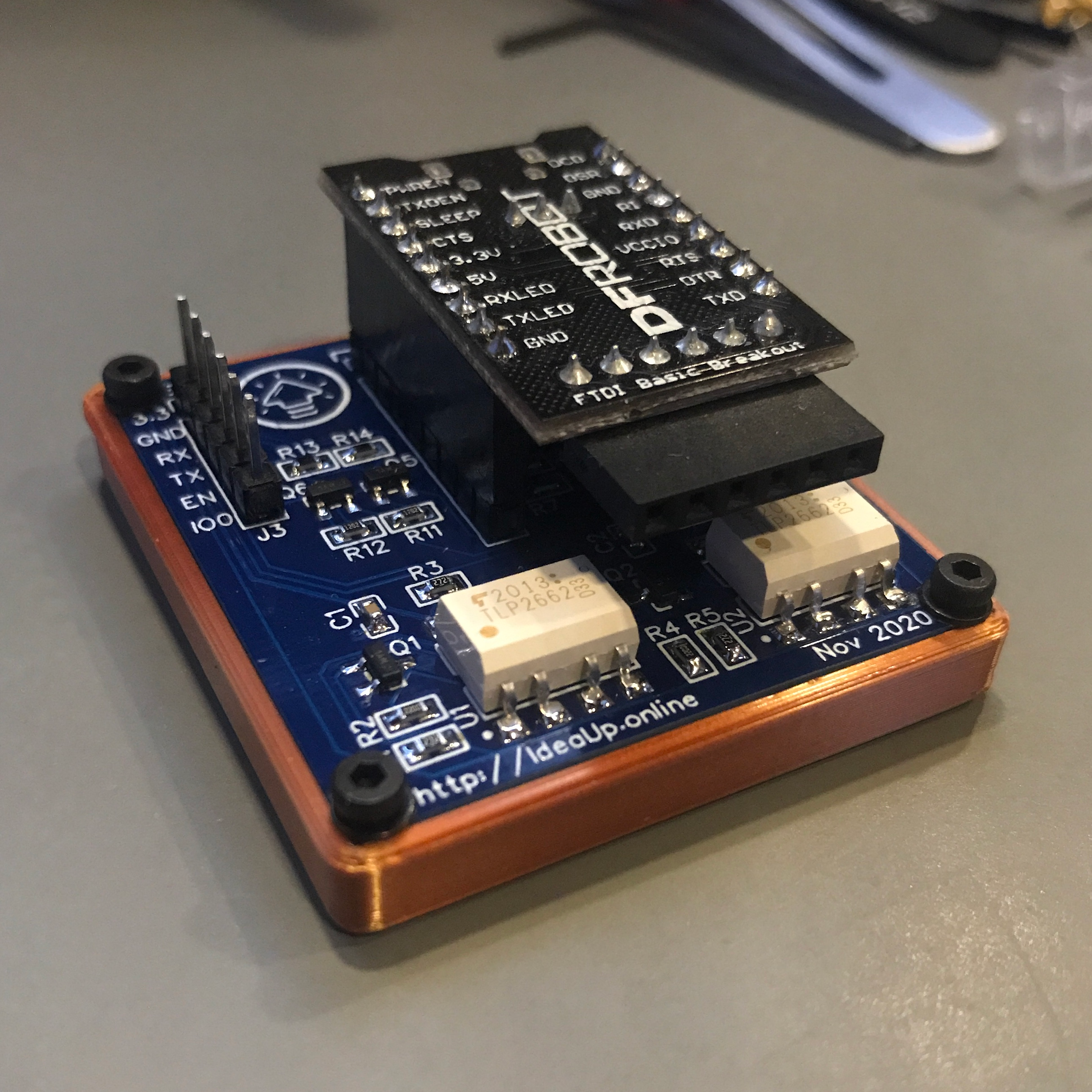
If you’re reading this then you’re probably an electronics hobbyist like me. So, you’ve been googling information and watching videos like I do. One name comes up over and over…JLCPCB.
It really sounds too good to be true, and that combined with the onslaught of advertising made me skeptical I have to admit. In the end, my skepticism was unfounded. I received ten copies of my board in about a week for US$16.80.

But that’s the end of the story…we need to go back to the beginning.
A Solution in Search of a Problem
I had decided I wanted to see how this worked, but the first challenge was that I didn’t have anything to make.
Fate intervened, as fate often does. In the meanwhile I was working on a different project. I had an ESP32 dev board on a breadboard being powered independently from my computer. Connecting the USB tied these systems together electrically and was causing headaches, but…I still wanted the communication with the computer to make debugging easier.
I had a DFROBOT FTDI Basic Breakout board kicking around, so I put it on another breadboard with some optoisolators. This worked out perfectly, allowing me to have my proverbial cake and eat it, too. Yum!
Even better, because the DFROBOT board breaks out all the required signals, I was also able to find a circuit that allows the computer to automatically put the ESP32 into programming mode when running a build. Because what good is a cake without icing?
With that, I had a simple but useful circuit for a first board attempt.
From Breadboard to Schematic
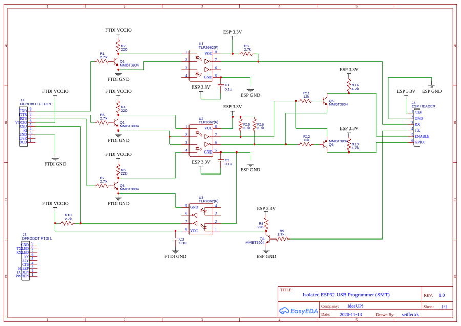
What I didn’t have was a schematic, so it was time to create that. In the spirit of keeping things simple, I decided to use EasyEDA for this, which is JLCPCB’s electronic design automation (EDA) suite.
With some fumbling around I was able to bang out a schematic, despite having zero experience going in. EasyEDA was, in fact, quite easy to get started with.

There are probably better ways to accomplish this with fewer parts, but that’s ok. In this case more parts is a feature in a way because it means more to route. Which means more routing challenges along the way, or put another way, more learning opportunities.
One little trick I learned here is that if you have two grounds and you want EasyEDA to keep them separate, you simply give them different labels. They become separate nets.
Also note that this is not a high-voltage isolation layout. The two sides are not physically isolated enough for that. It’s good enough to eliminate my ground loop and get some experience with PCBs though.
The transistors Q5 & Q6 and their associated parts do the magic of automatically programming an ESP32 module. This was found on the internet somewhere. I tried to retrace my steps to find the original source I used, but I could not. There are dozens of examples out there.
The rest of the transistors are simply inverters to flip the signals before the optoisolators flip them again. Weeeee!
Finally a few pull-up resistors and bypass caps and that’s all she wrote.
What a Rat’s Nest
Once I had the schematic, it was time to turn it into a PCB. This is simple, just choose Convert to PCB from the Design menu.

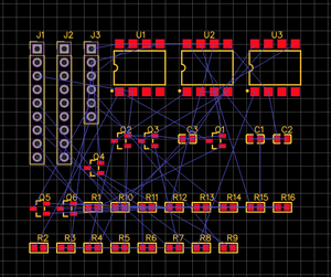
EasyEDA dumps you into a new board. This mess is appropriately called a rat’s nest, with the blue lines being rat wires. Because engineers love puns.
From here the job is to create a board outline and start dragging components into place.
The rat wires show you which pads need to be connected by traces. As each trace is drawn in the rat wire continues to connect the end of the trace to its ultimate destination, like a little GPS to keep everything on course. It’s easy to add vias and change which layer you’re drawing on. You will likely need to go back and forth to the schematic to get all the footprints correct as I did. And you have to be careful…I accidentally swapped the silk screen labels for two resistors, leading to boardy-no-worky until I figured it out and swapped the physical resistors.
I won’t go into a lot of detail here as there are plenty of routing tutorials out there. My favorite so far is Dave Jones’ EEVBlog YouTube channel. The advice in his videos was pivotal to the success of this board.
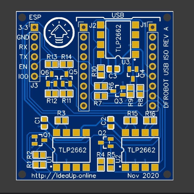
At any point during editing you can get a render of your board. Choose either 2D View or 3D View from the View menu.

Make it Real
The last step is to order the thing of course. Choose PCB Order from the Fabrication menu, and follow the prompts to quote and place the order. They have a very detailed order progress tracker on their website. It’s exciting to watch your project move from one process to the next. I received my boards in almost exactly a week to the southwest United States, despite not paying for upgraded shipping.
You will need the parts to populate the board, and you can even order them at the same time as the board from LCSC, the parts branch of JLCPCB. I didn’t use this service because I already had a bunch of the parts on hand. The remainder were added to a Mouser order that was already in progress.
Summary
All in all I was quite pleased with my JLCPCB experience. Their EDA suite was easy to use and their fully automated quoting and ordering system appealed to my introverted nature. Apparently they’ve worked with nerds and understand our needs. Kudos, JLCPCB, kudos…